Description
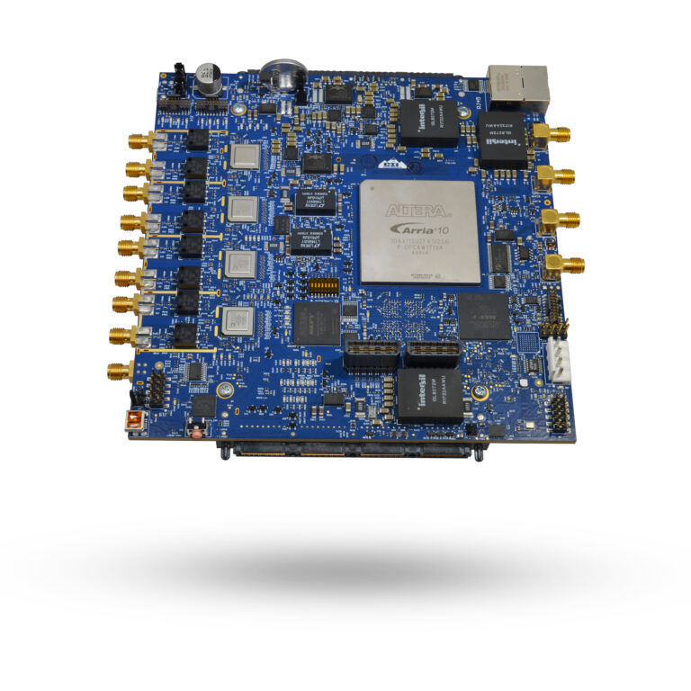
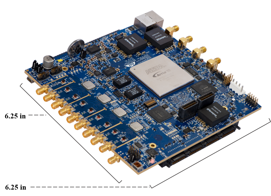
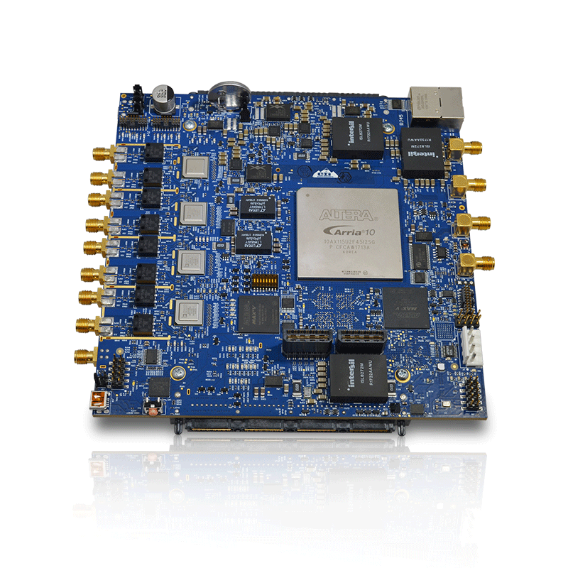
The 3DR-A10-ADC-250MSPS, known as Lightning III, is an 8-channel, 16-bit, 250 MSPS analog-to-digital converter board for digitizing and processing analog inputs. High performance, low latency processing can be implemented via the on-board Altera Arria 10 FPGA (10AX115U2F45I2SG).
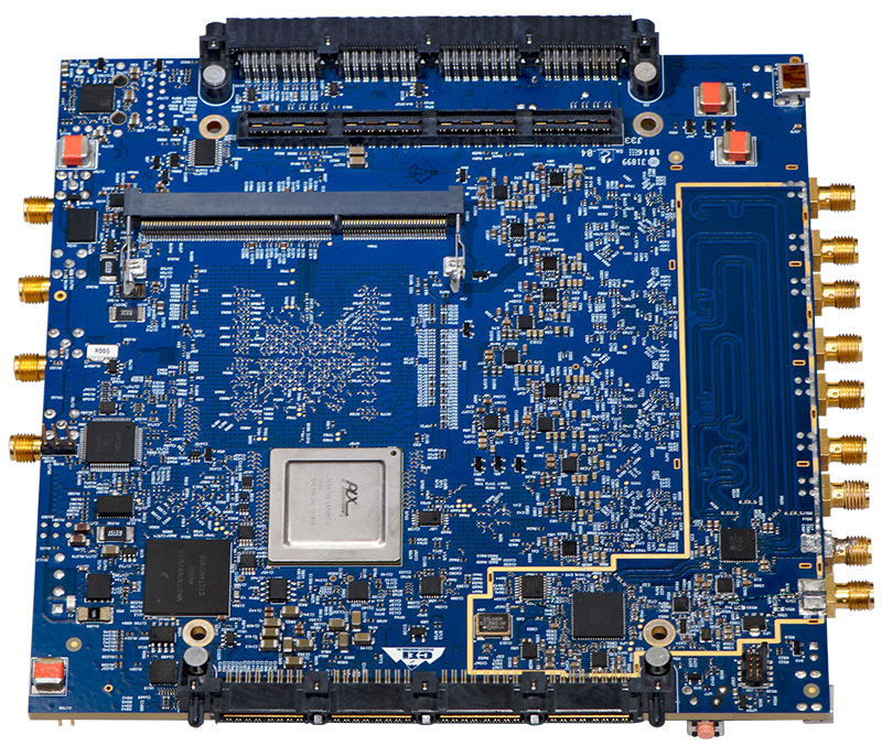
As with all 3DR computing modules, Lightning III supports three-dimensional connectivity, allowing the user to stack and/or tile modules to address a wide variety of processing, I/O, size, weight, and power requirements. Lightning III provides PCIe and LVDS interfaces via the Y and Z connectors to other modules in the 3DR computing family. It also offers additional external interfaces including SMA connections for clocking and triggering flexibility.
3DR computing technology brings together high performance computing, ease of programmability, low-cost, and commercial I/O flexibility in a modular, open systems and standards architecture to realize uniquely scalable and widely configurable, high speed embedded processing solutions for the development of radar, EW, SIGINT, and communication systems. 3DR computing possesses the unique ability to morph in size, shape, and processing capacity. This flexibility provides a low cost, standard solution capable of rapidly conforming to the vastly different power, space, and environmental requirements found aboard any surface, sub-surface, or airborne system or platform.
Applications
- Digital signal processing/data acquisition
- Radar receiver (digital receiver)
- Digital array processing and beamforming
- Electronic warfare/attack systems
Features
FPGA
- Altera Arria 10
- 10AX115U2F45I2SG
- 4GB DDR
Analog-to-Digital Conversion
- ADS42JB69
- 250 MSPS
- 16-bit
External I/O Support Available Via
- Y-connector (2x)
- Z-connector (1x)
- JTAG
- 4x—40 GbE daughter card
- SMA
- UART
Tailored Clocking and Triggering Flexibility
- Sample gates (SMA) in/out
- Trigger (SMA) in/out
- Clock inputs (SMA)
- On-board clock
Standard 3D Computing
- K61 microcontroller interface
- Controls power-on and power-down sequencing
- Monitors voltages and report faults over I2C bus
- Monitors current, e-fuse shut-down, and reports over I2C bus
- Monitors board temperature over I2C bus (external sensor available)
- On board EEPROM for data storage and logging (write protect available)
- FPGAs and CPLDs programmable over JTAG bus (for applicable modules with FPGAs and CPLDs), or via connectors from other 3DR computing boards (firmware required)
Benefits
- Enough FPGA Flash memory to hold two FPGA configurations
- On board circuitry fuse and temperature monitoring for board protection
- Standard 4-pin power
Specifications
ADC
- 250 MSPS
- 16-bit
Environmental
- Operating temperature: 0° to 50°C (commercial configuration)
- Storage temperature: (est) -55°C to 100°C, cooling airflow recommended, FPGA application dependent (heat sink mounts available)
Health Monitoring
- Board voltages
- PCIe switch, FPGA
- Two external temperature sensors
- I2C
- Smoke/impact detection
Clocking Options
- On board oscillator
- Off board SMA
Memory-DDR
- 4 GB unbuffered
External Interfaces*
- Y1, Y2, Z2 connectors: PCIe, LVDS (FPGA), and SerDes
*Connectors Y1, Y2, Z2 have PCIe, SerDes, and LVDS
Physical
- Dimensions: 6.25”L x 6.25”W
- Distance between board (stacked, board-to-board): 1.1”
Power
- Power consumption: 12V @ 15.5 amps (subject to FPGA loading)
- Supply options: 12V power cable
- Additional power features: e-fuse/continuous power monitoring
*C1, C2